Resources
 Part of the Oxford Instruments Group
Expand
Collapse
Part of the Oxford Instruments Group
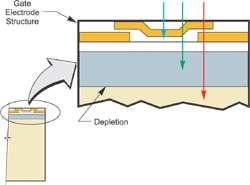
Cross-section of a typical CCD detector
The Spectral Response (or QE) of the CCD is governed by the ability of the photons to be absorbed in the Depletion Region of the detector. It is only in the depletion region that photons are converted into electronic charges and subsequently can be held by the electric fields which form the pixel. The charge held in the depletion region is then transferred and measured. To highlight the spectral response effects lets examine the cross- section of a typical CCD detector shown in diagram above.
Photons falling on the CCD must first transverse the region dominated by the gate electrodes by which the applied clocking voltages create the electric fields that form the boundary of the depletion region and shift charge through the CCD.
The gate structures can absorb or reflect all wavelengths to some extent and as a result reduce the spectral response below the theoretical maximum of 1 electron charge generated per one photon (in the case of visible light). The shorter wavelengths (blue light) are particularly absorbing and below ~350nm they absorb all the photons before they can be detected in the depleted region. Photons with longer wavelengths (i.e. red photons) have a low probability of absorption by the silicon and can pass through the depletion region without being detected and hence reduce the red sensitivity of the device. Photons with wavelengths greater than 1.1µm do not have enough energy to create a free electron charge and so they cannot be detected with Silicon CCD's.
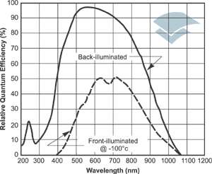
The various absorption effects combine to define the spectral sensitivity of the CCD. The spectral sensitivity is typically expressed as a QE Curve, in which the probability to detect a photon of a particular wavelength is expressed as a percentage.So for example if one in every 10 photons is detected this is expressed as a QE of 10%. The curve for a typical CCD is shown in the graph above.
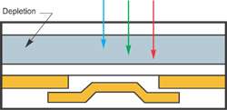
Back-Illuminated CCD
The losses due to the gate electrode structure can be completely eliminated in the Back-Illuminated CCD. In this design, light falls onto the back of the CCD in a region where the bulk of the silicon has been thinned by etching until it is transparent (a thickness corresponding to about 10-15 microns).
Back-thinning results in a delicate, relatively expensive sensor that, to date, has only been employed in high-end scientific-grade CCD cameras. Numerous attempts have been made to increase sensitivity more cost effectively by decreasing the absorption of the gate electrodes. The more successful attempts have included using less obstructive gate electrodes structures such as Open Electrode or Virtual Phase Technology (proprietary technology of Texas Instruments) or using more transparent gate electrodes such as Indium Tin Oxide in the Kodak™ Blue Plus™ technology.
Explore further in our Learning Centre.
© Oxford Instruments 2024