Resources
 Part of the Oxford Instruments Group
Expand
Collapse
Part of the Oxford Instruments Group
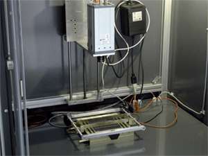
Figure 1 - The experimental setup for electroluminescence measurements. The cell is placed underneath the camera and electrically contacted from both sides.
The determination of luminescence in solar cells is an important characterization tool. Typical solar cells often have defects which limit the efficiency or lifetime of the cell. Many of these defects can be visualized with luminescence imaging, so by using this technique the manufacturing process can be optimized to produce better cells.
Luminescence imaging takes advantage of the radiative inter-band recombination of excited charge carriers in solar cells. The emitted photons can be captured with a sensitive CCD camera to obtain an image of the distribution of radiative recombination in the cell. This distribution is determined by the local excitation level, which allows the detection of electrical losses and can e.g. be used to map the diffusion length of minority carriers [1]. As the emitted light is of very low intensity and in the near infra-red, the camera must have a high sensitivity in the wavelength range of 900 to 1100 nm and little thermal noise. The Andor iKon-M BR-DD camera meets all of these demands, at a very suitable resolution of 1024 x 1024 pixels.
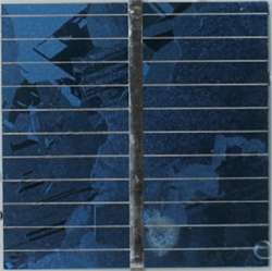
Figure 2 - Visual image of a solar cell in a laminated module.
The whole setup is surrounded by plastic sheets, allowing no ambient light to enter. The camera is placed above the samples on a linear stage to allow for different display windows, making measurements of samples sized 2 x 2 up to 21 x 21 cm2 possible. The objective lens can be fitted with spacer rings for detailed close up images. For electroluminescence images, the solar cells are supplied via their metal contacts with an external excitation current by a programmable power supply, while the camera takes an image of the emitted photons. Typical exposure times are in the range of 1 to 60 s. The power supply can deliver defined currents or voltages in all four quadrants of the IV characteristic, which allows for luminescence images with combined electric and optic excitation in the future.
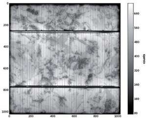
Figure 3 - Electroluminescence image of a multicrystalline 12:5 x 12:5 cm2 cell at 20mA/cm2 excitation current density and an exposure time of 1 s.
Electroluminescence imaging can be used to detect a multitude of defects in crystalline silicon solar cells, for example cracks, grain boundaries, broken contacts and shunts [2]. It can also yield absolute mappings of serial resistance [3] and diffusion length [1]. In figures 2 and 3 a photograph and the electroluminescence image of one multicrystalline 3 x 3 cm2 cell out of a laminated lab prototype module are shown. The electroluminescence image clearly shows a crack in the left half of the cell, which is not visible in the photograph. This crack was introduced while laminating the module and reduces the current of the whole module by ~25%. The effects of series resistance can also be seen in figure 3, as the radiation intensity decreases along the contact fingers towards the borders of the cell and in the area between these fingers. Figures 4 and 5 show the same cell, with exposure times of 1 s and 10 s (Note the different count scales). The difference in quality is very small, showing that the camera can deliver high quality images even at the short exposure times required for inline measurements in solar cell mass production.
© Oxford Instruments 2024