Resources
 Part of the Oxford Instruments Group
Expand
Collapse
Part of the Oxford Instruments Group
Nanoscale structures (quantum dots and quantum wires) are being studied extensively with a view to building ever more exotic devices, such as more efficient lasers and LEDs, or quantum information processing components. One type of material under investigation consists of semiconductor quantum wires based on InAs.
These are being explored because of their near-infrared optical properties. Work reported by Dr Benito Alén and co-workers on fundamental studies of isolated InAs nanowires (QWRs) identifies novel behaviour based around the metal-insulator transition in correlated electron systems. They made use of NIR photoluminescence (NIR-PL) to explore the transition dependencies on both excitation power and temperature.
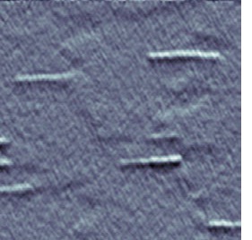
Fig 1: AFM image of the investigated QWRs (Courtesy Dr B Alén, CSIC, Madrid)
The analysis of the photoluminescence of individual semiconductor quantum wires is an invaluable tool to investigate the role played by attractive and repulsive Coulomb interactions among electrons and holes confined to one dimension. In these systems, the electronic and optical properties change dramatically depending on the number of trapped carriers, but the effect on the emission spectrum can be obscured if many QWRs with different sizes contribute to the emitted light. To ascertain the physics behind and confront the experimental data against existing theories, the photons emitted from just one QWR must be examined using high spatial resolution techniques and high sensitivity light detectors. This approach has been demonstrated for InAs/InP QWRs emitting at 1.5 µm, by researchers in Spain at the Consejo Superior de Investigaciones Científicas (CSIC) and the Universidad de Valencia.
The prediction of low threshold for laser emission, reduced temperature sensitivity, and slow surface recombination velocity has largely motivated the research on III-V semiconductor QWRs for optoelectronic applications in recent years. Among them, selfassembled InAs/InP QWRs can get their spontaneous emission tuned beyond 1.6 µm and their areal density reduced down to a few QWRs per square micron. They are therefore ideal candidates for the fabrication of advanced light sources in the telecom spectral region, and for the study of novel semiconductor physics. As for the latter, collective phenomena of one-dimensional excitons have been directly investigated in these nanostructures using NIR microphotoluminescence (µ-PL) techniques at low temperature, at the Universidad de Valencia and published by B. Alén et al. in Physical Review Letters
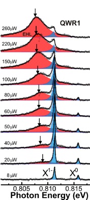
Figure 2. Typical single QWR emission spectra measured at 5 K with increasing excitation power . (Courtesy Dr B Alén, CSIC, Madrid)
The system consisted of a fibre-based confocal microscope arrangement inserted in the exchange gas chamber of an immersion liquid He cryostat. Excitation light from a 950 nm diode laser was brought into the microscope through a single mode optical fibre whose core acted as the excitation pinhole. The laser light was focused onto the sample through an objective lens (NA=0.55) producing a diffraction limited spot at the excitation wavelength. Light emitted by the few QWRs present in the excitation spot (see AFM image in figure 1) was collected by the same objective and focused onto a different optical fibre which in turn was connected at its opposite end to a spectrometer equipped with a TE cooled Andor iDus InGaAs (DU490A-1.7) camera. The faint light emitted from the individual QWRs could be detected using exposure times of 10 to 100 seconds thanks to the multichannel detection capabilities of the iDus InGaAs array and low dark current of the cooled array. The samples were made using self-assembly methods of epitaxially growing InAs structures on InP (001) substrates under conditions which preferentially led to the formation of QWRs rather than quantum dots (QDs). Reflection highenergy electron diffraction (RHEED) and Atomic Force Microscopy (AFM) analyses were used to characterize the morphology and aspect ratio of the individual QWRs. These structures were typically 20 nm wide and 200 nm long, corresponding to aspect ratios of ~1:10. Experiments were carried out to investigate how the samples behaved with variation in the excitation power, with powers as low as 8 mW up to 260 mW. They also investigated the temperature dependence.
Typical examples of µ-PL spectra collected on a single QWR as a function of excitation power density are depicted in figure 2. Due to the quantum confinement size effect, the different sized QWRs can emit at different energies, but they show a similar trend with the increasing photo-generated carrier density. The analysis of the lineshape of several spectral features observed at low and high excitation allowed a detailed study of the metal-insulator transition governed by enhanced Coulomb correlations in these systems. At low powers the sharp spectral feature at ~0.812 eV (~1528 nm) dominated whilst at high powers the broad spectral feature centred at ~0.807 eV(~1538 nm) dominated. This change in PL emission, induced by changes in carrier density, was indicative of the metal-insulator transition. The spectra show that the insulating excitonic gas (associated with high energy peaks – blue) condenses into a metallic-like electron-hole liquid phase (associated with the low energy band - red), with an increase in carrier density.
Novel behaviour on the metal-insulator transition within a correlated electron system, as realized in single InAs/InP QWRs emitting in the NIR, was clearly demonstrated by Alén and co-workers. They developed techniques based on µ-PL, which allowed exploration of the carrier interactions and its dependence on photo-excitation powers and temperature. These fundamental studies will underpin future developments of ever more exotic devices such as high efficiency micro-/nano- lasers and LEDs.
Acknowledgment
Appreciation is gratefully extended to Dr Benito Alén, IMM-CSIC, Madrid and Prof. Juan Martinez Pastor, Universidad de Valencia, Spain.
References
1) D. Fuster, B. Alén, L. González, Y. González and J. Martínez-Pastor, “Initial stages of self-assembled InAs/InP(0 0 1) quantum wire formation”. Journal of Crystal Growth 301 (2007), 705.
2) L. J. Martínez, B. Alén, I. Prieto, D. Fuster, L. González, Y. González, M. L. Dotor, and P. A.Postigo, “Room temperature continuous wave operation in a photonic cristal microcavity laser with a single layer of InAs/InP self-assembled quantum wires”, Optics Express 17 (2009), 14993.
3) B. Alén, D. Fuster, G. Muñoz-Matutano, J. Martínez-Pastor, Y. González, J. Canet-Ferrer and L. González, “Exciton Gas Compression and Metallic Condensation in a Single Semiconductor Quantum Wire”, Phys. Rev. Lett. 101 (2008) 067405.
© Oxford Instruments 2024