
iDus 420 CCD
View Product
 Part of the Oxford Instruments Group
In the field of scientific-grade CCD detectors, back-illuminated CCDs and Electron-Multiplying EMCCDs offer key benefits for applications where the photon signal available is extremely low. Such applications include low-light cell microscopy and fast chemical mapping. This article presents one of the key challenges associated with the use of back-illuminated CCDs for Near-Infrared (NIR) detection, namely optical etaloning. Optical etaloning is where internal reflection occurs between the edges of the depletion region, creating interference effects in spectra. We discuss the technology of fringe suppression and other strategies to overcome this.
Introduction
The ability of a CCD camera to capture photons and ‘detect’ the associated ‘photoelectrons’ that are generated is typically measured in terms of signal-to-noise ratio (SNR). The SNR can be expressed as follows:
Where
It is clear that achieving high SNR depends not only on careful minimization of the different sensor noise sources (cooling for the dark noise, slower readout speed and/or use of electron multiplying gain for the readout noise, fast vertical clocking for CIC), but also on high sensor QE.
Back-illumination of CCDs – the attraction of high Quantum Efficiency in the Visible and NIR Regions
The QE of a CCD is governed by its ability to absorb incoming photons in the photosensitive silicon also know as the depletion region. It is only in this region that photons are converted into electron-hole pairs, which are then confined by means of electric fields into a ‘pixel’. The charges held in these pixels can then be read out.
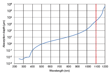
Figure 1: Absorption depth in Silicon at 300K as a function of incident photon wavelength
Shorter wavelength photons (blue light) are absorbed closer to the silicon surface, while longer wavelength photons can travel deeper into the silicon matrix before being absorbed. Photons with wavelength above 1.1 μm do not have enough energy to create an electron-hole pair and so cannot be detected: a silicon CCD is effectively transparent at these longer wavelengths.
Figure 1 shows the absorption depth of photons as a function of wavelength in crystalline silicon.

In front-illuminated CCDs, incoming photons must first transverse a polysilicon electrode structure and a silicon oxide (SiO) insulating layer (see Figure 2). The electrode structure can absorb and reflect part of the incoming photon flux before it reaches the photosensitive region. This region is also referred to as the depletion region (it is deplete in mobile charge carriers) and has the ability to capture and store the electrons generated from the photon signal.
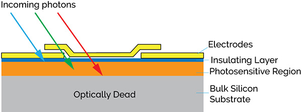
Figure 2: Typical front-illuminated CCD (cross section)
This absorption in the surface layers is extremely pronounced in the ultraviolet (<350 nm), resulting in near zero detection for UV photons. This design structure also limits the QE of front illuminated devices to ~50% in the visible region.
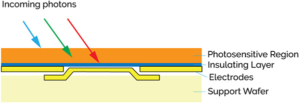
Figure 3: Typical back-illuminated CCD (cross section)
In order to eliminate the losses incurred at the front surface, a back-illuminated (BI) configuration can be adopted. The back-illumination process involves the removal of the bulk silicon substrate by mechanical grinding and chemical etching, allowing direct exposure of the active photosensitive region to the incoming photons as shown on Figure 3. These devices can exhibit peak QE’s of up to 95% with appropriate anti-reflection (AR) coatings. NIR QE of standard back-illuminated CCDs can be further enhanced by the use of a thicker photosensitive region, also referred to as the deep depletion region. Material with higher resistivity is used in these devices.
The thicker photosensitive region offers a greater absorption path to longer wavelength photons, and subsequently lowers the probability for these photons transversing the whole way across the active region (refer to Figure 1).
The higher resistivity material allows the electric fields, created by applying voltages to the electrodes to penetrate the entire depth of the now thicker photosensitive region and hence better collect and confine photoelectrons within the pixels.
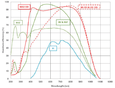
Figure 4: Typical QE performance at +25ºC of front-illuminated (‘FI’), back-illuminated visible-optimized (‘BV’), UV-enhanced backilluminated (‘BU2’), back-illuminated deep-depletion CCDs with NIR AR-coating (‘BR-DD’) and broadband dual AR-coating (‘BEX2-DD’). The new BI Low Dark Current Deep-Depletion (‘LDC-DD’)[4] and ‘BRDD’ have identical QE characteristics.
These devices are known as back-Illuminated, deep depletion (BI-DD) CCDs.
A property of back-illuminated CCDs that is often overlooked is their propensity to generate constructive and destructive optical interference when illuminated with coherent photons. The outer surfaces of the depletion region are highly reflective and form a cavity where internal reflection takes place. This is optical etaloning. This behavior is especially pronounced in the NIR and can lead to signal modulation as high as 40%. This highly undesirable effect can be extremely disruptive for applications based on NIR Raman, NIR photoluminescence or Bose Einstein Condensate (BEC) studies.
Front-illuminated CCDs however, do not suffer from optical etaloning. In these devices, incoming photons with longer absorption lengths (longer wavelengths) do not encounter any interface with highly mismatched refractive indexes after reaching the photosensitive region. These photons have therefore a very low chance of being reflected back-and-forth in the depletion region to create interferences. Photons that are not absorbed in this region are lost in the optically dead bulk silicon substrate.
The following section describes the origin of the interferometer behavior of back-illuminated CCDs, by comparing their structure with a particular type of interferometer called a Fabry-Pérot étalon.
The ultra-thin cavity formed by the depletion region, with parallel and highly reflective surfaces is akin to a Fabry-Pérot étalon configuration.
Back-illuminated CCDs and analogy to the Fabry-Pérot étalon
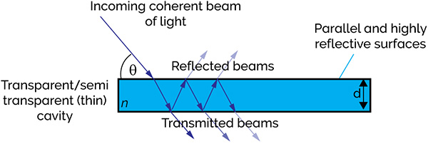
Figure 5: Typical Fabry-Pérot étalon configuration
A typical Fabry-Pérot étalon consists of a thin, transparent optical medium with two flat, parallel and highly reflective surfaces. A back-illuminated CCD is similar to this configuration, with the depletion region sandwiched between a silicon oxide insulating layer and air / vacuum with highly mismatched refractive indexes which create highly reflective interfaces. Coherent light entering the cavity can undergo multiple reflections, which can lead to the generation of destructive and constructive interference, largely determined by the Etalong configuration in terms of its thickness or 'optical length’, and the dielectric properties of the material within it. This is illustrated in Figure 7.
The modulation characteristics of the signal are governed by the following equation (adapted from [iii]):
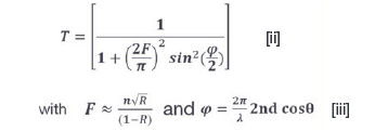
Figure 6 shows the influence of the cavity Finesse on the quality of the étalon.
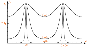
Figure 6: Influence of cavity Finesse on fringing sharpness and amplitude (integers p and p+1 refer to consecutive fringes separated by one roundtrip through the cavity)
Etalons with highly reflective surfaces (high R, hence high Finesse) show sharper transmission peaks, while etalons with less reflective surfaces (low R, hence low Finesse) lead to increasingly smeared fringes.
The spacing in wavelength between two successive transmitted optical intensity maxima of a Fabry-Pérot étalon is given by the free spectral range (FSR). Typical FSR values for back-illuminated CCDs are shown below:
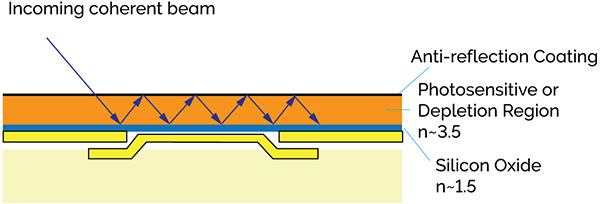
Figure 7: Back-illuminated, sensor and étalon cavity structure analogy (n refers to the refractive index)
Spectral and spatial etaloning in back illuminated CCDs
The thickness of the depletion region in back-illuminated CCDs can typically vary between 10-50 µm (type-dependent). The absorption length of NIR photons in silicon can be several times this thickness (see Figure 1), which effectively means that the CCD is semitransparent at these wavelengths. The CCD depletion region has a refractive index of ~3.5, while the silicon oxide (insulating) layer has a refractive index of ~1.5. This significant mismatch means that this interface is extremely reflective, so that NIR photons entering the depletion region and reaching the insulating layer without being absorbed will be reflected back towards the front surface of the depletion region. These reflected photons can in turn reach the front surface of the active region. This front surface is typically AR-coated in order to minimize the refractive index mismatch at the silicon-air interface. This increases the transmission of photons through this interface and consequently limits further potential internal reflections in the active silicon region.
However since AR coatings are not perfect, longer wavelength photons can undergo several reflections back-and-forth in the depletion region, and under conditions dictated by the cavity characteristics create destructive and constructive interferences. These multiple reflections increase the chance of NIR photons being absorbed and therefore increase the QE of the sensor in the NIR. The interference pattern linked to the wavelength-selectivity of the étalon is referred to as spectral fringing. Since the surfaces of the depletion region are not perfectly parallel or flat, local variations of a few µm of the depletion region thickness can change the interference conditions and alter the spectral fringing pattern. This effect is referred to as spatial fringing. The detected fringing pattern on a CCD is a combination of both spectral and spatial contributions. The combined effects of spectral and spatial fringing is illustrated in Figure 8 back-illuminated sensor (BV) optimized for the visible region.
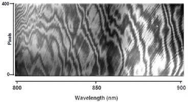
Figure 8: Un-binned image of a broadband tungsten lamp taken with a Shamrock 750 spectrograph and a back-illuminated visible-optimized iDus 420A-BV
For spectroscopy applications, multiple wavelengths are dispersed across the CCD sensor width: the subsequent fringing pattern superimposed on the ‘normal’ signal will show the contribution of each interfering wavelength. The AR coatings applied to the front surface of the depletion region are specific to a particular wavelength range. Outside the range of greatest efficiency, the Finesse of the cavity is affected, resulting in a gradual decrease of fringe sharpness and intensity. Note: single NIR coatings applied to back-illuminated, deep depletion CCDs are typically optimized at around 800 nm, bringing the peak QE to ~95% at this wavelength.
Influence of cooling temperature
Cooling is used to minimize thermally generated ‘dark noise’ contribution in CCDs in order to maximise SNR. The latest generation of thermo-electric (TE) based scientific cameras can achieve sensor temperatures down to -100°C.
Cooling also has an influence on the photon absorption depth in crystalline silicon, changing the refractive index of the active region [2], while also inducing small mechanical changes in the active silicon structure. This means that the étalon characteristics also change with temperature, resulting in temperature-dependent constructive and destructive interference patterns as illustrated on Figure 9.
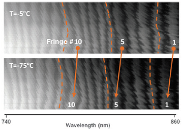
Figure 9: Un-binned images of broadband tungsten source captured with a back-illuminated visible-enhanced Newton DU971-BV EMCCD at different sensor cooling temperatures. Camera was coupled to a Shamrock 750 spectrograph. Fringes are identified by a number to facilitate visualization of the shift with temperature.
Maintaining a stable cooling temperature is therefore strongly recommended when dealing with relative or absolute intensity data correction, where such changes in the sensor characteristics and interference pattern will have an impact on the baseline data taken with the standard calibration source.
Minimizing etaloning in back-illuminated CCDs
Interference patterns in back-illuminated CCDs can never be totally suppressed, but can be reduced through a range of techniques highlighted here.
Front-illuminated CCDs do not suffer from optical etaloning. In these devices, incoming photons with longer absorption lengths (longer wavelengths) do not encounter any interface with highly mismatched refractive indexes after reaching the photosensitive region. These photons therefore have a very low chance of being reflected back-and-forth in the depletion region and create interferences. Photons that are not absorbed in this region are lost in the optically dead bulk silicon substrate.
Several approaches can be used to minimize etaloning in the NIR for back-illuminated CCDs:
All of these methods are sensitive to the way light is coupled onto the CCD and to the sensor temperature.
Table 1 highlights the effectiveness of the fringe suppression process for different types of back illuminated CCDs. It should be noted that this process intrinsically can have large variations within it.
| BI Deep-Depletion without fringe suppression | BI Deep-Depletion with fringe suppression | BI visable enhanced without fringe suppression | BI visable enhanced with fringe suppression | |
| Peak modulation in the NIR | > 10% | 1-5% | 20-40% | 10-20% |
Influence of vertical binning
The modulation amplitude will also depend on the number of pixels binned on the sensor. Figure 10 shows a number of binned continuous broadband spectra in 2 binning configurations: (i) Full Vertically Binning (FVB) on a 3.2 mm high sensor, and (ii) a 16-row high binned track in the middle of the same sensor. Spectral profiles are for (a) a ‘standard’ back-illuminated CCD without fringe suppression (BV) and, (b) a back illuminated with fringe suppression (BVF): both sensors are optimized for the visible region.
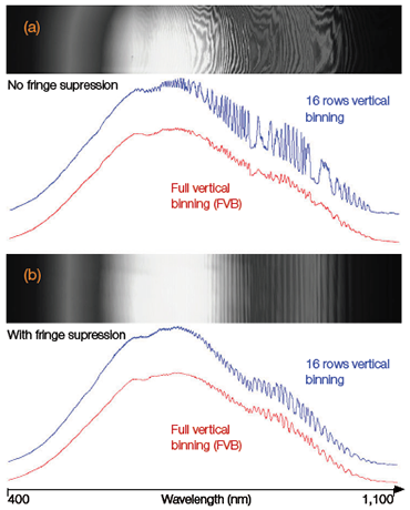
Figure 10: FVB spectra (red) and 16-row high binned track spectra (blue) of a broadband tungsten source acquired with a ‘standard’ back-illuminated CCD (a), and a back-illuminated CCD with ‘fringe suppression’ (b) attached to a Shamrock 750 spectrograph. Corresponding un-binned images are shown above each dataset.
The following observations can be made:
Back-Illuminated deep-depletion CCDs – High NIR QE and Low etaloning
BI-DD sensors boast typical peak QE up to 95% in the NIR (see Figure 4), which makes these devices the platform of choice for low light NIR detection. But the other great advantage of such sensors is the extremely low etaloning exhibited in the NIR.
The thicker photosensitive region of BI-DD sensors offers a greater absorption path for longer wavelength photons, which minimizes the chance for multiple reflections of NIR photons occurring inside the étalon-like photosensitive region structure. This consequently greatly reduces the detected signal modulation in the NIR. In order to further reduce this signal modulation, sensor manufacturers apply a ‘Fringe-suppression’ process described in previous section.
Figure 11 illustrates the signal modulation in BI-DD CCDs. It clearly shows the much reduced fringing pattern on both image and vertically binned spectra compared to thinner back-illuminated CCDs (see Figure 10).
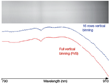
Figure 11: FVB spectra (red) and 16 rows high binned track spectra (blue) of a broadband tungsten source acquired with a back-illuminated deep depletion CCD attached to a Shamrock 750 spectrograph.
Summary
References
© Oxford Instruments 2024