iStar sCMOS
View Product
 Part of the Oxford Instruments Group
Particle Imaging Velocimetry (PIV) is an optical method of flow visualization used in research and industry to obtain velocity measurements and related properties in fluids. By taking two closely spaced images or ‘snapshots’ of the species, and using correlation algorithms, it is possible to build up 2D and 3D dynamic flow maps [1].
The key to successful measurements is capturing short pulses of scattered light from the species (or tracers added to it) within a well-controlled timescale on the order of a few 100s of nanoseconds to a few microseconds typically. Generally PIV requires a high sensitivity detector that offers accurate timing schemes in terms of triggering capability. This technical note details how the new Andor iStar-sCMOS camera may be integrated into a system to facilitate relatively easy and successful PIV measurements.
Among the different approaches for making PIV measurements, two of the main ones can be summarised as:
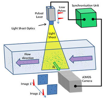
Figure 1: Schematic of the main components of a typical PIV setup.
Typically micron-sized particles act as the light scatterers for imaging. These are sometimes intrinsic to the species but often trace or ‘seed’ particles are added into the species which are chosen to act as excellent scatterers at the laser wavelength being used. Good signal strength is important in the more challenging applications where the generation of real-time velocity flow maps are needed with particle flows up to and beyond supersonic speeds. Temporal separation or ‘resolution’ is a very important performance parameter. Key to this working well is the accurate synchronization of the laser (or flash lamp) to the operation of the camera.
The Andor iStar-sCMOS is an intensified sCMOS (ISCMOS) camera which offers flexible and accurate triggering or timing capability, making it straight forward to configure into a PIV experiment using either approach indicated above.
Typical applications of PIV include studies on, turbulence within air flows, turbidity, water flow, blood flow in the body, combustion studies and even in the simulation of avalanches [2]. A number of variants of the technique of particular note are, Stereoscopic PIV and Scanning PIV – both of which enable the capture of 3D volume vector maps, and Micro-PIV (µPIV) – where analysis is carried out on the microscopic scale using microscopes, a good example being micro-fluidics [1].
Andor Solis or the Andor Software Development Kit (SDK3) acquisition software may be used to configure, control and run the acquisition process for the capture of the image data. It is also possible to use 3rd party acquisition software environments such as LabView or MatLab. For PIV applications, the iStar-sCMOS camera features the 5.5 megapixel sCMOS sensor, the only sCMOS device offering true global shutter operation at full frame rates of up to 50 image-frames per second (fps) [3]. The global shutter exposure functionality is utilized in a PIV double-exposure configuration, which offers an ‘effective inter-exposure-frame’ or inter-image time down to < 1 µs.
Detailed in this document is how the iStar-SCMOS may be configured and incorporated in typical PIV setups. It outlines key assumptions or requirements to be aware of at the outset, some configurations used, and how to optimize the relative timings through the application and control of well synchronised trigger pulses.
A schematic of the main components needed in a common setup for PIV is shown in figure 1. The required parts include:
As shown in figure 1, a thin fantailed sheet of illumination of the laser light is produced with special optics – often incorporating a cylindrical lens. The illuminated plane through the sample is imaged with full field-of-view (FOV) on to the camera. Synchronisation of the relative timing of the laser and camera system is achieved with a master timing control unit. This synchronisation unit choreographs with trigger pulses, by varying their delays and pulse widths, the firing of the laser and the optimised acquisition of the images.
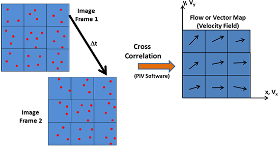
Figure 2: Generation of the Vector map by Image Processing with specialist PIV software.
The camera is configured to acquire a pair of exposures of the sample plane with minimal time delay between the exposures; a series of multiple exposure pairs can also be acquired using longer kinetic series. When the two images in a PIV image-pair are captured, special PIV software using correlation algorithms is used to build up the vector map. The time separation, Δt, between the images of a pair is referred to as the ‘inter-image’ time. This process is illustrated in figure 2.
The length of the camera exposure, i.e. the exposure time of the sCMOS sensor, is normally not a key requirement, with relatively long exposures commonly being used. It is the gating of the intensifier part of the camera, and/or the triggering of the laser along with its pulse-length that determines, a) the effective exposure time of each image acquired, and b) the time gap (Δt) between the two images in a PIV image-pair.
Depending on what type of light source (pulsed laser, strobe or flash lamp), that is being used with the iStar-sCMOS, a number of possible triggering arrangements may be used. If a pulsed laser is used with this camera, a configuration could be used where the synchronisation unit sends a pre-trigger to the camera to initiate the exposure cycle of the sCMOS sensor, then it sends two delayed pulses to the intensifier (defining the acquisition ‘window’ widths and spacing), and it sends several pulses to the laser. Synchronisation delays are adjusted such that the first laser pulse will coincide with the first intensifier gate: this should generally occur near the end of the exposure of the first image-frame. The second laser pulse, synched with the second intensifier gate, should occur early in the exposure of the second image-frame.
A simple schematic of these relative timings is illustrated in figure 3. The figure shows timing pulses which go high and low with time. The key timing parameter is the time, Δt, between the illumination pulses (and/or gating pulses), as this determines the temporal separation gap of the two images.
A key advantage of an intensified SCMOS camera arises in the situation where a CW or quasi-CW light source is used; in this case the gating of the intensifier can be used to define the ‘effective exposure time’ (gate pulse width) of the images and the separation time, Δt, between the image-frames in a PIV pair, though one has to take into account, and be aware of the decay time of the phosphor used within the intensifier tube when working with the shortest inter-image times. This is discussed in some detail later in this technical note.
Referring to figure 3, this shows a train of external trigger pulses being delivered from the synchroniser to the camera; in this schematic the trigger is derived from the rising edges. The exposure time for the sCMOS sensor and its response to the external triggers is given by the SCMOS FIRE pulse, which goes high when the sensor is being exposed and goes low for data transfers at the readout phase of the sensor.
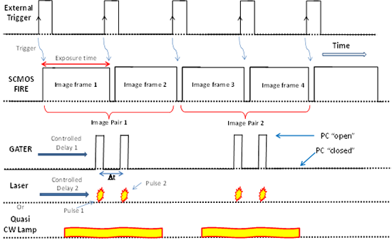
Figure 3: Simple schematic showing the relative timing of trigger pulses used to sync the laser with camera and have the images captured in two successive exposure frames of the sCMOS sensor. The SCMOS FIRE pulse shows the exposure of the sCMOS sensor for each frame. Two illumination scenarios are illustrated – either the use of a pulsed laser or a quasi-CW flash lamp.
Pulses to the laser and the intensifier Gater electronics are generated by the synchroniser, which uses appropriate control delays for each set of triggers to synch image acquisitions on the SCMOS sensor with the laser and intensifier. The Gater shows the triggering being delivered to the photocathode (PC) of the intensifier with the intensifier being responsive (PC-“open”) whilst this pulse is high and unresponsive (PC-“closed”) when low. Note that the laser pulse pairs and/or triggering of the intensifier only occurs at every other transition between image frames i.e. the delivery of pulse pairs will be at half the frequency of image frame rate. Two illumination schemes are included – either a pulsed laser or a quasi-CW source could be used in this type of setup.
At this point it is worth summarising some key requirements for PIV experiments with the shortest temporal ‘resolution’ (separation) and the fastest frame rates. It is essential that the following applies:
These requirements are assuming a sequence of ‘image-pairs’ are to be acquired at the fastest rate, with the minimal temporal gap (down to sub-microsecond) between the images within any given pair.
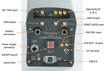
Figure 4: Picture showing the connections to the camera for handling triggering and communications.
There are a number of different configurations of the triggering and operation modes of the camera which can be used for PIV measurements. Figure 4 shows the various hardware connectors or terminals on the back of the camera and figure 5 illustrates the software interface. In the following discussion some familiarity with the ISCMOS manual [2] is assumed. (A useful summary of the key terms and definitions used is given below)
For each configuration case, the following software/system settings are generally recommended for the iStar-sCMOS,
Settings relating to the sCMOS sensor part:
Settings relating to the intensifier part:
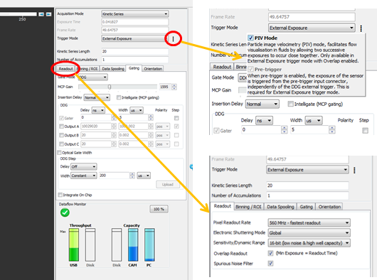
Figure 5: Screenshot of the software interface on the iStar-sCMOS camera.
It is useful to consider the timing diagram for a given setup as a means to understanding the triggering involved in making an acquisition. Figure 6 illustrates a detailed timing diagram for a setup consistent with the outlined settings above. Specifically, in this example the gating mode is assumed as set in GATE ONLY and a synchronising unit is controlling the triggering of the laser and camera with a number of its output trigger channels.
The schematic (not to scale) shows how the rising and falling edges of the trigger pulses evolve over time relative to each other; time is displayed on the horizontal axis. In the top half of the figure, timings are shown for the sCMOS sensor part of the system (ARM, FIRE and Charge Transfer), in the middle is the intensifier (Gater), and in the bottom half are the timing triggers for the laser, with an optical schematic of the laser pulses. In this example a twin head Q-switched laser is the assumed illumination source, and the triggers for generating the laser pulses are denoted as QSW1 and QSW2. Note in the real dual laser there will also be triggers earlier in time to activate the flash lamps but these are omitted here in the interest of simplification.
The following is offered in way of explanation of the timings (refer to figure 6):
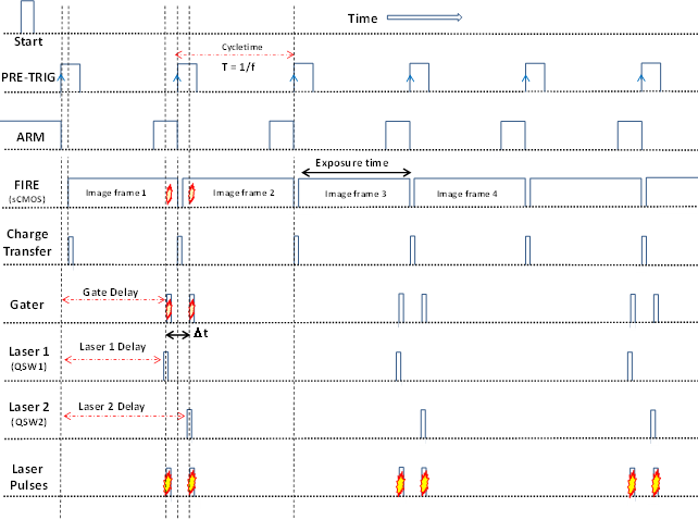
Figure 6: Schematic timing diagram showing the evolving TTL trigger pulses for controlling the acquisition of PIV image-pairs. Settings based on Global Shutter with External Exposure and Overlap Mode On; intensifier gated using DIRECT GATE; laser pulses generated by delivering Q-switches to twin laser heads; synchronisation triggers from external unit.
As well as the standard external triggering input (via EXT TRIG), the iStar-sCMOS has been designed with an alternative external triggering input – the PRE-TRIG input, which offers flexible de-coupling of the triggering to the sCMOS sensor relative to the DDG board of the intensifier. This has been primarily supplied for use with the External Exposure Acquistion mode, and it allows for the triggering of the sCMOS sensor earlier in time relative to the intensifier under the control of an external synchronisation unit. When one considers the insertion delays within the camera electronic paths, there is a signicant delay in the response time of the sCMOS sensor relative to the intensifier. In some cases this can be easily handled with using the delay within the DDG to increase the delay to the intensifer relative to the sCMOS sensor, or alternatively adjusting delays externally in the external synchronisation unit. However, there are situations, for example when using certain lasers, when the minimum insertion delay to the intensifer is desireable. This is where the new added feature of the PRE-TRIG input presents significant benefit.
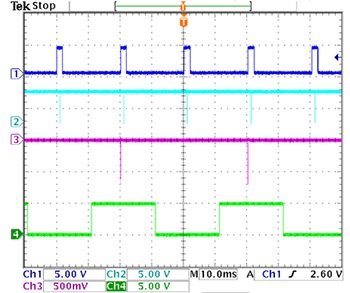
Figure 7: Screenshot from an oscilloscope showing sample traces in the setting up of a PIV measurement. Note the timescale is on a coarse setting of 10 ms/div in this example. 1: EXT TRIG, 2: FIRE, 3: GATE MONITOR, 4: ARM.
When External Exposure is selected, with Overlap mode ON, every positive rising edge of an external input TTL pulse will trigger the end of one exposure and the start of a new exposure, with the period of the external trigger pulses defining the exposure cycletime. The exposures will be separated by the electronic ‘charge transfer’ time (2 µs) or ‘inter-exposure’ gap – see figure 6. Note that, if the period of the external trigger pulses is less than the minimum exposure time possible, some positive rising edges (triggers) will be ignored. For the most stable performance in terms of having the same exposure period throughout a sequence of acquistions, the external trigger period should be set, if possible, to match the possible exposure cycletimes.
Whilst the minimum ‘inter-exposure-frame’ time is limited to 2 µs electronically, it is possible to achieve ‘effective’ optical transition times of the the order of ~300 ns or less. This can prove useful when the shortest ‘inter-image’ times (Δt) are needed; a detailed explanation is presented in a later section of this note.
To assist with the setting up and optimisation of timings, it useful to display the pulses on an oscilloscope. The ARM, FIRE, and Gater (using Gate Monitor connection) are accessible from the back and side of the camera (see figure 4), and the external triggers can be coupled to easily. Figure 7 shows a screenshot from an oscilloscope showing sample traces which may be useful when setting up a PIV experiment.
Terms and parameters used in the technical discussion are described here. Reference is also made to the connections on the back of the camera as illustrated in figure 4 and to the iStar-sCMOS manual [4].
There are two distinct ways that the exposure time will be determined depending on whether Overlap Readout Mode is switched ON or OFF.
a) If Overlap mode is set to ON, the exposure time of the sCMOS sensor will be determined by the rising edge of successive external trigger pulses, with the first rising edge starting the exposure and the successive rising edge ending the exposure (and so on if in a multiple acquisition sequence).
b) If Overlap mode is set to OFF, the exposure time will be set by the rising and falling edges of each individual external trigger pulse, with the rising edge starting the exposure and the falling edge ending it: by varying the duration (pulse-width) of each external pulse one can control the ‘exposure’ time.
Detailed timing information for the 5.5 MegaPixel iStar-sCMOS camera operating at the fastest readout rate of 560 MHz and minimum cycletime is illustrated in figure 8. A summary of the timing values is given in Table 1. This shows clearly the relationship between the rising edges of the external trigger and the transition between image frames when in External Exposure mode. Note that by using smaller regions of interest (ROI) or smaller fields-of-view within the sensor area, one can achieve much faster frame rates -refer to the specification sheet [3].
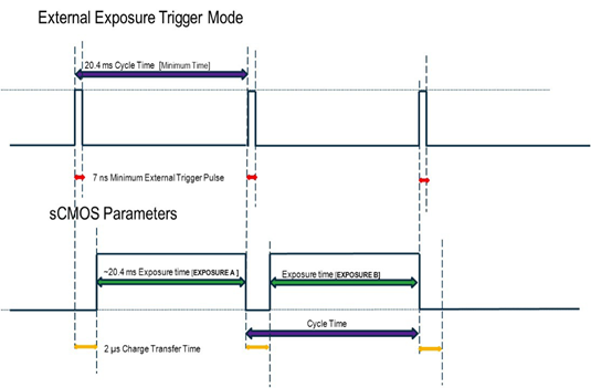
Figure 8: Schematic of the timings for the sCMOS sensor of the iStar sCMOS when operated in External Exposure Trigger Mode, with OVERLAP readout mode ON, maximum readout rate of 560 MHz, and minimum Cycletime for a full image at the minimum possible exposure.
| Parameter | Time |
| Inter-Exposure-Frame or Charge Transfer time | 2 µs |
| Minimum Cycletime | 20.4 ms |
| Minimum Exposure time | 20.4 ms |
| Frame read time (Full Frame) | 9.98 ms |
| Row read time | 9.24 µs |
| Minimum External trigger pulsewidth | 7 ns (2 clock cycles) |
| Minimum Gatewidth | 2 ns |
One of the challenges when setting up the timing for a PIV measurement with a series of acquisitions is the synchronisation of the capture of each image-pair relative to the main frame rate, where the frame-pairs are captured at half the rate of the main frame rate (see figure 3, 6, 7). To help simplify the triggering scheme and the demands on the external synchronisation unit, a special feature referred to as ‘PIV mode’ in the software has been incorporated for use with the DDG. This offers (optional) selection of a particular trigger pattern for the ARM pulse. In this case the ARM is programmed to accept only every second pulse from the main trigger source and reject the in-between triggers. As indicated earlier and in the information of Table 1, triggers are only accepted by the DDG when the ARM is high.
The configuration of the camera is as before with External Exposure, Overlap ON, and a trigger connection to PRE-TRIG. However, since the DDG is being used a trigger connection is needed on the EXT TRIG input of the camera. The DDG allows for accurate internal control of the gate pulses in delay and width to both the photocathode of the intensifier and the output control triggers A, B and C. Figure 9 shows a detailed timing scheme utilising this feature.
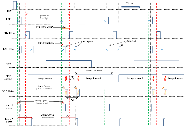
Figure 9: Timing scheme illustrating the use of the ‘PIV’ mode option (with External Exposure) to control the DDG such that only every second of the main trigger pulses actually triggers the photocathode.
A master timing/synchronisation unit, once receiving a START, generates its pre-configured reference frequency of triggers, REF, and through a number of independent channels delivers triggers with appropriate delays to the PRE-TRIG, EXT TRIG and the light source – in this case the Q-switches for a dual head laser for illustration purposes. The synchroniser is programmed to provide to the EXT TRIG a double trigger pulse for each reference (REF) trigger; the separation of the EXT TRIG pulses delivered to the DDG determines the inter-image spacing and their width defines the ‘effective exposure time’. As can be seen in the figure, the ARM is programmed to only go high for alternate sets of trigger pulses to the DDG. It is worth noting that the above configuration could be implemented with two Stanford DDG SR535 boxes. An alternative scheme where only one external delay generator is required is outlined in Appendix A for reference.
Note in this timing scheme the ability to control the delay of the PRE-TRIG pulse enables the REF trigger associated with every ‘inter-exposure’ transition to be used to generate the corresponding EXT TRIG pulses to the DDG. This offers great advantage in terms of reducing the magnitude of relative delays required for synchronisation resulting in significantly reduced jitter being associated with any of the trigger pulses.
External Exposure triggering ensures a wide variety of sequences can be easily set up, allowing the user to select their own optimal mode of operation. Figure 10 shows a selection of external trigger sequences for different camera configurations. In the figure the top trace represents the external trigger pulses, shown relative to the individual acquired images in the bottom trace. This exposure pattern directly relates to the FIRE pulse. The images are identified with ‘A’ or ’B’ and a number, to indicate their position within the image-pair and the sequence respectively. This illustrates only a subset of all the possible arrangements that could be configured.
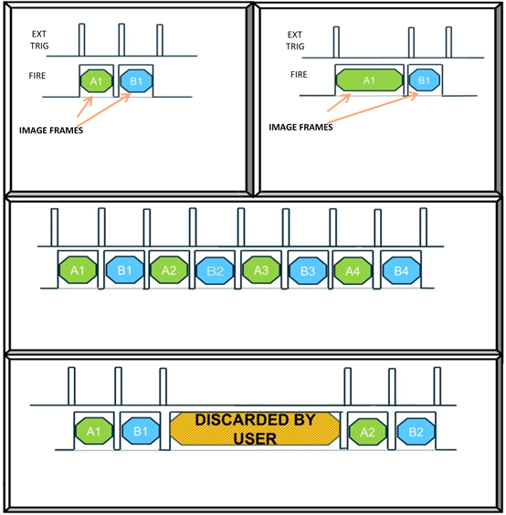
Figure 10: Examples of acquisition sequences of paired images using External Exposure Mode with Overlap On: a) a single image-pair with the period of the external trigger matched to the exposure time of the camera, b) a pair where there is variation in the period of the external triggers, c) a kinetic series of image-pairs and, d) a series of frame pairs with a gap in between i.e the external triggers are delivered in bursts.
Generally in a PIV experiment it is desirable to minimize the time separation between the successive images within a pair and to have the sharpest non-blurred images possible. This can be achieved with a pulsed laser as the illumination source that can deliver short duration pulses spaced close together in time. Alternatively the gating of the intensifier of the iStar-SCMOS camera can be used to capture an optical image-pair by sending two closely spaced trigger pulses (controlled in width and separation) to the photocathode. This section will look closely at how the camera system – sCMOS sensor and intensifier - can be optimised and used to achieve the smallest inter-image times and consequently the minimum temporal separation or ‘resolution’ when capturing an image-pair. As alluded to earlier it is possible to acquire images with closer temporal spacing than the minimum electronic transition time between exposures of 2 µs. To understand the minimum time possible and the limitations on it, there are two important characteristics of the system that must be considered:
The former allows the spacing of ‘image’ pulses to go below the 2 µs transfer gap, whilst the latter poses the lower limit on how close the ‘image’ pulses can be spaced in time.
A standard approach for acquisition of an image-pair is to capture the first laser pulse (image) at the end of the first exposure cycle and the second pulse (image) at the beginning of the second exposure (see figure 11(a)). What will follow will demonstrate how the performance can be enhanced to significantly reduce the inter-image separation, Δt, as illustrated in figure 11(b). Firstly we will consider the influence of the phosphor decay and then what we will refer to as the ‘optical’ inter-exposure transition.
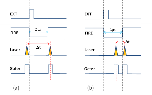
Figure 11: Schematic showing the temporal spacing within an acquired PIV image-pair when operating in external exposure mode. Shown in (a) is the normal setup used with the laser and gater pulses bridged across the inter-exposure transition gap, and (b) illustrating the possibility of closer spacing utilising the ‘optical’ transition time and, bringing the laser and/or gater pulse into the inter-exposure gap.
The phosphor contained within the intensifier, and which converts the amplified and gated electron signal from the photocathode back to an optical signal suitable for detection by the sCMOS sensor, has a characteristic decay time. This optical signal is observed to fall off exponentially over a significantly longer time than the actual gatewidth for the signal collected. This does not compromise the actual temporal or spatial resolution but does have implications when two events are captured close together in time, where the elongated decay profile could lead to crosstalk between the two captured events or images. Crosstalk just refers to some signal from one event or image leaking through into the other event or image. The iStar sCMOS offers a choice of phosphor materials, P43 for best signal response and P46 for shortest temporal profile: the decay times (to the 10% reference levels) of P43 and P46 phosphors are ~2 ms and ~200 ns respectively [3]. Whilst the P43 phosphor offers greater efficiency in terms of signal level produced, the faster decay of the P46 phosphorescence allows for closer temporal spacing of the illumination events. Therefore one should choose the P46 phosphor option for the most demanding PIV applications where the temporal separation of events has to be less than 2 ms. By the same token the decay time of the P46 phosphor does place a lower limit on how close the events can be spaced in time to >200 ns. A schematic of this decay profile is illustrated in figure 13.
Up to this point the focus has been on the electronic triggering and the minimum electronic inter-exposure-frame time of 2 µs. However, when the optical response of the sCMOS structure is considered it is evident that smaller inter-image delays or pulse separations may be accessed. The characteristic optical response of the sCMOS sensor in the inter-exposure region is shown in figure 12. This was produced by scanning a single short laser pulse across the inter-exposure gap by varying the relative delay between the laser pulse and the FIRE pulse. This relative delay is referenced to the rising edge of the FIRE pulse after the inter-exposure transition (‘0’ delay). The averaged signal intensity captured in the two image frames are compared as delay (horizontal axis) is varied across the gap. Superimposed on the graph is the temporal profile of the electronic signal (FIRE) for the inter-exposure gap with its 2 µs width.
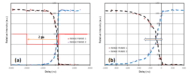
Figure 12: Characteristic of the optical response of the sCMOS structure in the region of the inter-exposure gap. The inter-exposure-frame transition or gap is schematically shown in (a) and an enlarged view of the optical transition is shown in (b). The red squares (and black dashes) correspond to the integrated intensity in image-frame 1 and the crosses (and blue dashes) are for intensity in image-frame 2.
What is evident from this characteristic is that the optical response transition occurs over ~ 400 ns and that the edge of the transition lies within ~100 ns of the rising edge of the FIRE pulse to the right of the gap. It is apparent from the data that the time separation between images may be reduced beyond the electrical gap width of 2 µs to the order of several hundred nanoseconds. However, this extended PIV regime would require accurate control of the timing delays and jitter within the system for an optimised setup. Figure 13 shows a schematic of how the electrical and optical pulses would sit relative to each other in this scenario. As indicated earlier another important factor to be borne in mind is the elongated decay profile of the phosphor (see figure 13): the P46 phosphor would be chosen if operating in this regime.
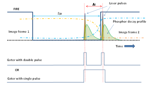
Figure 13: Schematic of the relative timings for both electrical and optical when operating in an extended PIV regime within the inter-exposure gap. Note that the decay time of the phosphor and the optical transition time of the sCMOS structure determine how close together the laser pulses and/or intensifier triggers may be in order to avoid crosstalk between the two images. Schematic representations of the relative intensity profiles are also superimposed for illustrative purposes.
When all these considerations are taken into account the closest temporal separation that can be achieved without the problem of crosstalk between images is ~300 ns and the delays need to be such that the second pulse of the laser and/or intensifier comes just after the rising edge of the FIRE pulse at the start of the second image-frame.
Note - it is strongly recommended that if the user wishes to operate in this extended PIV regime that the optical transition characteristic is generated first as this will ensure all delays in the electrical and optical lines are taken into account as well as the intrinsic characteristics of the camera. This is relatively easy to do by several means, such as using,
As illustrated in figure 13 when a pulsed laser is being used to define the two temporal windows for the images the intensifier may be gated with two synched gater pulses or one longer gater pulse which bridges the laser pulses.
In conclusion to this note it is worth listing the key benefits offered by the iStar-SCMOS camera for PIV.
The question may arise as to whether there are any benefits to using an intensified sCMOS camera if a pulsed laser source is being used in any case, for example when a standard sCMOS camera can be used for PIV measurements [5]. However, there are a number of very important benefits with an intensified sCMOS camera and these may be summarised as:
As indicated earlier this technical note should be read in conjunction with the camera manual and specification sheet. For further information and guidance on setting up and using the iStar-SCMOS camera, please contact the Product Management team at andor.oxinst.com
Illustrated here is a basic timing scheme for PIV using the functionality of the DDG (with PIV mode selected) of the iStar-sCMOS camera and one external delay generator (Stanford SR535) (refer to figure A1). In this arrangement the external unit is configured to generate at a master or reference frequency (REF) bursts of two pulses.
This reference frequency is generated internal to the external delay unit. The two pulses in a burst are spaced in time to correspond to the desired inter-image-frame gap. This trigger pattern is delivered to a number of output channels where the delay for each channel can be varied independently (PRE-TRIG delay, EXT TRIG delay, Lamp delay). One set of triggers is sent to the PRE-TRIG of the camera where only the rising edge of the first pulse can be accepted as a valid trigger – the second pulse is ignored (as it falls within an exposure cycle). Similarly a train of double triggers are delivered to the EXT TRIG input of the camera where the acceptance of such triggers by the (internal) DDG is determined by the ARM pulse. As the ARM is only high for every second set of pulses, the DDG will only be triggered on alternate sets of pulses. This means that the acquisition of PIV frame-pairs will be at half the frequency of the main frame rate – as is desired. The actual width of the internal pulses to the intensifier is set within the software for the internal DDG (GATEWIDTH), as is the Gate Delay.
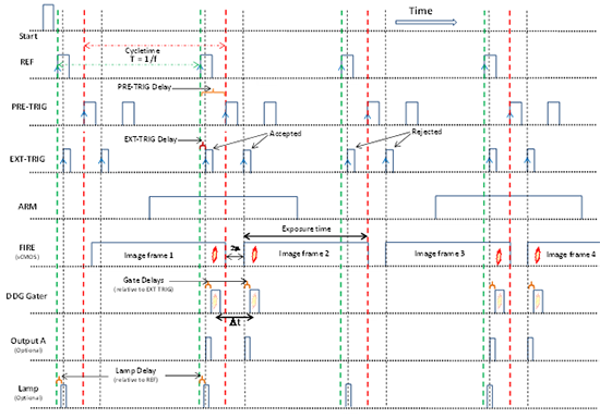
Figure A1: Timing scheme for PIV acquisitions using the ‘PIV mode’ in the External Exposure configuration that can be implemented with one external digital delay generator.
Also included is the output triggering for Output A. It is worth noting that the trigger outputs A, B and C are all available for triggering other parts of the experiment such as lamps, lasers, LEDs or shutters, though it must be remembered that these will have the same double pulse pattern as per the internal DDG Gater. If such pulses are not suitable and triggers are needed then the reference trigger REF can be used to supply independent pulses, for example to a laser as shown at the bottom of figure A1.
The following figures, A2 and A3, summarise the settings needed in the Solis software, and typical traces captured on an oscilloscope.
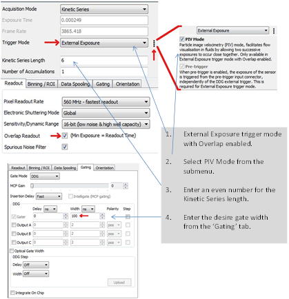
Figure A2: Screenshot from Solis software showing the settings for utilising the ‘PIV mode’ utility when operating in External Exposure mode.
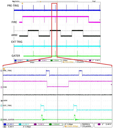
Figure A3: Screenshots of oscilloscope traces demonstrating the operation of the ‘PIV mode’ on the iStar-sCMOS. External DDG generator delivers -
1. PRE-TRIG pulses whose period determines exposure time of SCMOS. Second pulse in a burst is ignored.
2. EXT TRIG pulses
3. Only the two pulses of every alternate burst are accepted by the Gater
ARM controls the acceptance of external triggers
© Oxford Instruments 2024